TDS9099 BACKPLANE
This product is obsolescent and should not be used for
new designs with a long lifetime.
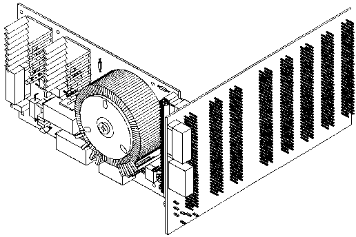 |
TDS990 Power supply and TDS9099 Backplane
|
This printed circuit board 183 x 102mm connects together the
wire-wrap pins of DIN connectors on the rear of a 42E (half 19") rack.
The board is pushed over the pins and is then soldered to them. Take care to
leave sufficient gap between the backplane and card-frame. There are positions
for 8 connectors (DIN 41612 type C, available separately). Each position has
two rows of 32 pins separated by 5.08mm. The rack positions and normal functions
are as follows (left to right as seen from the front of the rack):
|
Position
|
Function
|
|
3
|
User Application Board or TDS971 IEEE-488 board
|
|
7
|
User Application Board
|
|
11
|
User Application Board
|
|
15
|
User Application Board
|
|
19
|
User Application Board
|
|
25
|
User Application Board
|
|
29
|
User Application Board
|
|
34
|
TDS990 Power Supply
|
The TDS9092 (or TDS2020F) computer, TDS9096 13-bit A to D
boards, TDS973 Input/Outputs and the TDS961 PROM Programmer can be placed in
any of the user application board slots.
RACK SYSTEM NEEDED
Most Eurocard racks are suitable. We suggest the following
parts which make up a good-looking case which includes a rack. Order as CASE-FRAME:
Half-19" 3U Case Frame
Suitable front panel for above
16 Board guides for above
Note that you also need up to 8 wire-wrap sockets. Order them
under the part number SOCKETDIN64.
BACKPLANE CONNECTIONS
These lines connect all slots on the backplane except the TDS990
power supply position. The pins connected together are the address, data and
control buses, and the power lines. Other pins are left open to meet your own
requirements. Names and functions refer to the TDS9092. The star * indicates
active at 0V:
|
Position
|
Name
|
Dir
|
Description
|
|
a1
|
A14
|
Out
|
Address bus bit 14
|
|
a2
|
A12
|
Out
|
Address bus bit 12
|
|
a3
|
A10
|
Out
|
Address bus bit 10
|
|
a4-a13
|
A9-A0
|
Out
|
Address bus bits 9-0
|
|
a14-a21
|
D7-D0
|
I/O
|
Data bus bits 7-0
|
|
a22
|
E*
|
Out
|
Clock, inverse of E, 1.2288MHz
|
|
a23
|
R/W*
|
I/O
|
Read/Write for Motorola style chips
|
|
a24
|
WR*
|
Out
|
Write. For Intel style peripherals
|
|
a26
|
NMI
|
Inp
|
Non-maskable interrupt
|
|
a30
|
P56
|
I/O
|
Port 5 bit 6 or I2C clock out
|
|
a31
|
P57
|
I/O
|
Port 5 bit 7 or I2C data bus
|
|
a32
|
VIN
|
Inp
|
Power supply +6V to +16V
|
|
c1
|
A15
|
Out
|
Address bus bit 15
|
|
c2
|
A13
|
Out
|
Address bus bit 13
|
|
c3
|
A11
|
Out
|
Address bus bit 11
|
|
c15
|
SW+5V
|
Out
|
Switched +5V output. Controlled by 232ON and
232OFF . Use to switch off other circuits to save power.
|
|
c16
|
CS01C0
|
Out
|
Address 01C0-01CF decode. Positive active, strobed with
E. Use for LCDs.
|
|
c17
|
CS01B0*
|
Out
|
Address 01B0-01BF decode. Negative active, strobed with
E. Do not use when words INKEY or NEWKEY are used (needed internally)
|
|
c18
|
CS01A0*
|
Out
|
Address 01A0-01AF decode. Negative active, not strobed
with E.
|
|
c19
|
CS0190*
|
Out
|
Address 0190-019F decode. Negative active, not strobed
with E.
|
|
c20
|
CS0180*
|
Out
|
Address 0180-018F decode. Negative active, not strobed
with E.
|
|
c21
|
STBY*
|
Inp
|
Standby input (hardware control)
|
|
c22
|
E
|
Out
|
Clock, 1.2288MHz
|
|
c23
|
RESET*
|
I/O
|
Use as output to other logic, or as input to reset the
TDS9092 computer. Use does not clear the RAM as does power-up.
|
|
c24
|
RD*
|
Out
|
Read. For Intel-style peripherals
|
|
c26
|
P50
|
I/O
|
Port 5 bit 0 general purpose I/O or IRQ1* interrupt input
|
|
c27
|
P51
|
I/O
|
Port 5 bit 1 general purpose I/O or IRQ2* interrupt input
|
|
c28
|
P52
|
I/O
|
Port 5 bit 2 general purpose I/O or Memory Ready input
|
|
c29
|
P53
|
I/O
|
Port 5 bit 3 general purpose I/O or Halt* input
|
|
c30
|
P54
|
I/O
|
Port 5 bit 4 general purpose I/O or Input Strobe* input
|
|
c31
|
P55
|
I/O
|
Port 5 bit 5 general purpose I/O, or Output Strobe*
output
|
|
c32
|
GND
|
Gnd
|
Ground
|
USE OF BACKPLANE WITH TDS971 IEEE-488 BOARD
TDS9092 The addresses
0100-0117 are already used on the TDS9092 for internal RAM. Interchange the
signals to pins a4 and a5 of the TDS971 (address lines A8 and A9). This will
change the address of the board from 01xx to 02xx. On the TDS9099 backplane
there are links E and F which can be remade to interchange these lines to the
left position on the backplane.
TDS9092 & TDS2020F Make links G and H and unmake links
A and B. This will connect the +5V and -12V lines to the TDS971. Also unmake
links C and D so that pins c29 and a31 are not connected across the rack; they
have special functions on the TDS971.
|