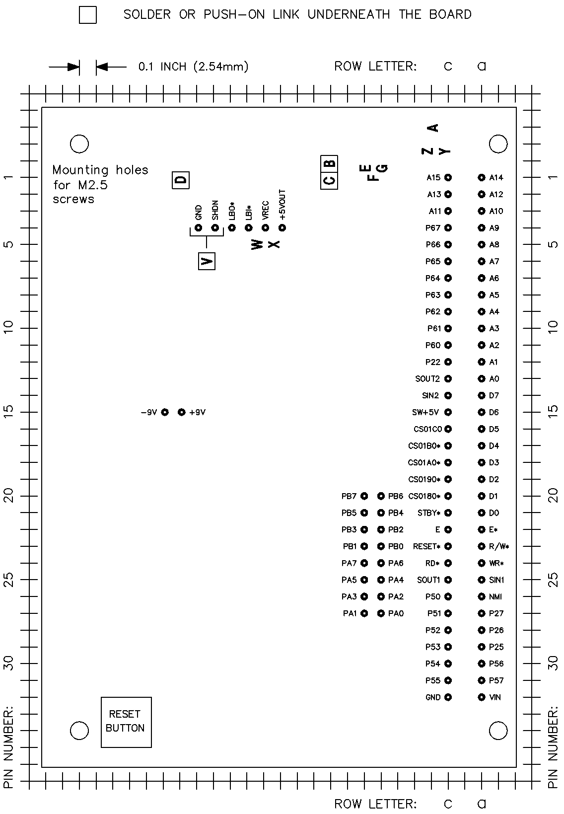
| Pin |
Name |
Dir |
Description |
| a1 |
A14 |
Out |
Address
bus bit 14 |
| a2 |
A12 |
Out |
Address
bus bit 12 |
| a3 |
A10 |
Out |
Address
bus bit 10 |
| a4 |
A9 |
Out |
Address
bus bit 9 |
| a5 |
A8 |
Out |
Address
bus bit 8 |
| a6 |
A7 |
Out |
Address
bus bit 7 |
| a7 |
A6 |
Out |
Address
bus bit 6 |
| a8 |
A5 |
Out |
Address
bus bit 5 |
| a9 |
A4 |
Out |
Address
bus bit 4 |
| a10 |
A3 |
Out |
Address
bus bit 3 |
| a11 |
A2 |
Out |
Address
bus bit 2 |
| a12 |
A1 |
Out |
Address
bus bit 1 |
| a13 |
A0 |
Out |
Address
bus bit 0 |
| a14 |
D7 |
I/O |
Data
bus bit 7 |
| a15 |
D6 |
I/O |
Data
bus bit 6 |
| a16 |
D5 |
I/O |
Data
bus bit 5 |
| a17 |
D4 |
I/O |
Data
bus bit 4 |
| a18 |
D3 |
I/O |
Data
bus bit 3 |
| a19 |
D2 |
I/O |
Data
bus bit 2 |
| a20 |
D1 |
I/O |
Data
bus bit 1 |
| a21 |
D0 |
I/O |
Data
bus bit 0 |
| a22 |
E* |
Out |
Clock,
inverse of E, 1.2288MHz |
| a23 |
R/W* |
I/O |
Read/Write
for Motorola-style chips |
| a24 |
WR* |
Out |
Write.
For Intel-style peripherals |
| a25 |
SIN1 |
Inp |
Main
serial port input, RS232 levels |
| a26 |
NMI |
Inp |
Non-Maskable
interrupt. Pull-up to +5V |
| a27 |
P27 |
Out |
Port
2 bit 7. Switched to 0 by 232ON and 1 by 232OFF |
| a28 |
P26 |
I/O |
Port
2 bit 6 or Timer Out 3 |
| a29 |
P25 |
I/O |
Port
2 bit 5 or Timer Out 2 |
| a30 |
P56 |
I/O |
Port
5 bit 6 or I2C clock out |
| a31 |
P57 |
I/O |
Port
5 bit 7 or I2C data bus |
| a32 |
VIN |
Inp |
Power
supply +6V to +16V (or 6V AC, see Fast Start Guide) |
| |
|
|
|
| Pin |
Name |
Dir |
Description |
| c1 |
A15 |
Out |
Address
bus bit 15 |
| c2 |
A13 |
Out |
Address
bus bit 13 |
| c3 |
A11 |
Out |
Address
bus bit 11 |
| c4 |
P67 |
I/O |
Port
6 bit 7 general purpose I/O |
| c5 |
P66 |
I/O |
Port
6 bit 6 general purpose I/O |
| c6 |
P65 |
I/O |
Port
6 bit 5 general purpose I/O |
| c7 |
P64 |
I/O |
Port
6 bit 4 general purpose I/O |
| c8 |
P63 |
I/O |
Port
6 bit 3 general purpose I/O |
| c9 |
P62 |
I/O |
Port
6 bit 2 general purpose I/O |
| c10 |
P61 |
I/O |
Port
6 bit 1 general purpose I/O |
| c11 |
P60 |
I/O |
Port
6 bit 0 general purpose I/O |
| c12 |
P22 |
I/O |
Port
2 bit 2 or serial clock in |
| c13 |
SOUT2 |
Out |
Second
serial port out, RS232 levels |
| c14 |
SIN2 |
Inp |
Second
serial port in, RS232 levels |
| c15 |
SW+5V |
Out |
Switched
+5V output. Controlled by 232ON and 232OFF . Use to switch off
other circuits to save power |
| c16 |
CS01C0 |
Out |
Address
01C0-01CF decode. Positive active, strobed with E. Use for LCDs |
| c17 |
CS01B0* |
Out |
Address
01B0-01BF decode. Negative active, strobed with E. Do not use when
keyboard words INKEY or NEWKEY are used (needed internally) |
| c18 |
CS01A0* |
Out |
Address
01A0-01AF decode. Negative active, not strobed with E |
| c19 |
CS0190* |
Out |
Address
0190-019F decode. Negative active, not strobed with E |
| c20 |
CS0180* |
Out |
Address
0180-018F decode. Negative active, not strobed with E |
| c21 |
STBY* |
Inp |
Standby
input (hardware control) |
| c22 |
E |
Out |
Clock,
1.2288MHz |
| c23 |
RESET* |
I/O |
Use
as output to other logic, or as input to reset the TDS9092. Use
does not clear the RAM as does power-up |
| c24 |
RD* |
Out |
Read.
For Intel-style peripherals |
| c25 |
SOUT1 |
Out |
Main
serial port output, RS232 levels |
| c26 |
P50 |
I/O |
Port
5 bit 0 or IRQ1* interrupt input |
| c27 |
P51 |
I/O |
Port
5 bit 1 or IRQ2* interrupt input |
| c28 |
P52 |
I/O |
Port
5 bit 2 or Memory Ready input |
| c29 |
P53 |
I/O |
Port
5 bit 3 or Halt* input |
| c30 |
P54 |
I/O |
Port
5 bit 4 or Input Strobe* input |
| c31 |
P55 |
I/O |
Port
5 bit 5 or Output Strobe* output |
| c32 |
GND |
Gnd |
Ground |
| |
|
|
|
| Pin |
Name |
Dir |
Description |
| PA0 |
PA0 |
I/O |
Port
A bit 0 general purpose I/O |
| PA1 |
PA1 |
I/O |
Port
A bit 1 general purpose I/O |
| PA2 |
PA2 |
I/O |
Port
A bit 2 general purpose I/O |
| PA3 |
PA3 |
I/O |
Port
A bit 3 general purpose I/O |
| PA4 |
PA4 |
I/O |
Port
A bit 4 general purpose I/O |
| PA5 |
PA5 |
I/O |
Port
A bit 5 general purpose I/O |
| PA6 |
PA6 |
I/O |
Port
A bit 6 general purpose I/O |
| PA7 |
PA7 |
I/O |
Port
A bit 7 general purpose I/O |
| PB0 |
PB0 |
I/O |
Port
B bit 0 general purpose I/O |
| PB1 |
PB1 |
I/O |
Port
B bit 1 general purpose I/O |
| PB2 |
PB2 |
I/O |
Port
B bit 2 general purpose I/O |
| PB3 |
PB3 |
I/O |
Port
B bit 3 general purpose I/O |
| PB4 |
PB4 |
I/O |
Port
B bit 4 general purpose I/O |
| PB5 |
PB5 |
I/O |
Port
B bit 5 general purpose I/O |
| PB6 |
PB6 |
I/O |
Port
B bit 6 general purpose I/O |
| PB7 |
PB7 |
I/O |
Port
B bit 7 general purpose I/O |
| |
|
|
|
| Pin |
Name |
Dir |
Description |
| -9V |
V |
Out |
Output
from DC-DC converter |
| +9V |
+9V |
Out |
Output
from DC-DC converter. Use with peripherals such as A to D |
| |
|
|
|
| |
|
|
|
| GND |
GND |
Gnd |
Ground.
Connected internally to c32 |
| SHDN |
SHDN |
Inp |
Shutdown.
This input must be shorted to ground for correct operation |
| LBO* |
LBO* |
Out |
Open
drain low battery output |
| LBI* |
LBI* |
Inp |
Leave
open circuit for Low Battery operation or use as input with LBO*
as inverted open drain output |
| VREC |
VREC |
Out |
Normally
same as VIN, but rectified DC output if powered from AC voltage
(see Fast Start Guide) |
| +5VOUT |
+5VOUT |
Out |
From
on-board regulator. Maximum 180mA including TDS9092's own consumption |