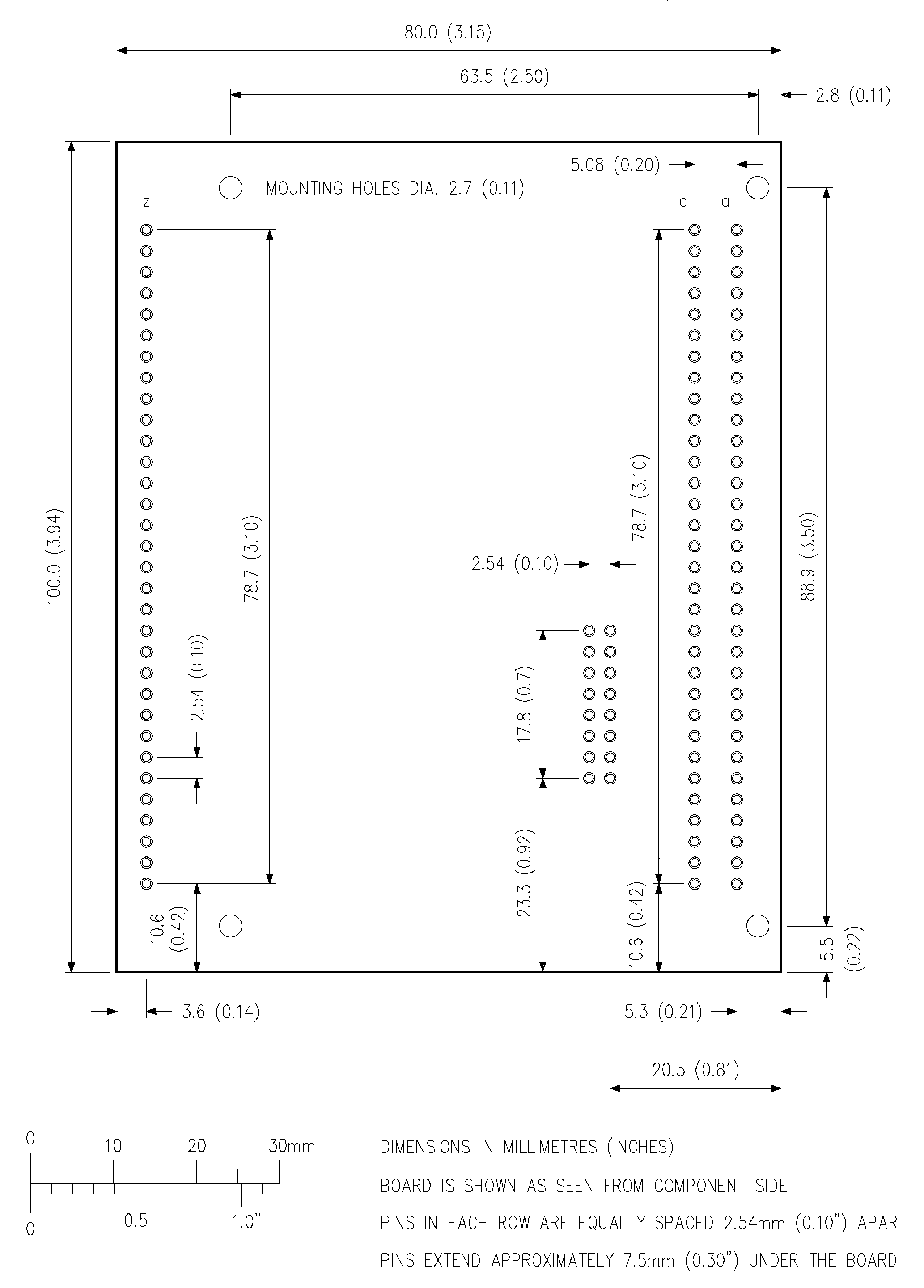
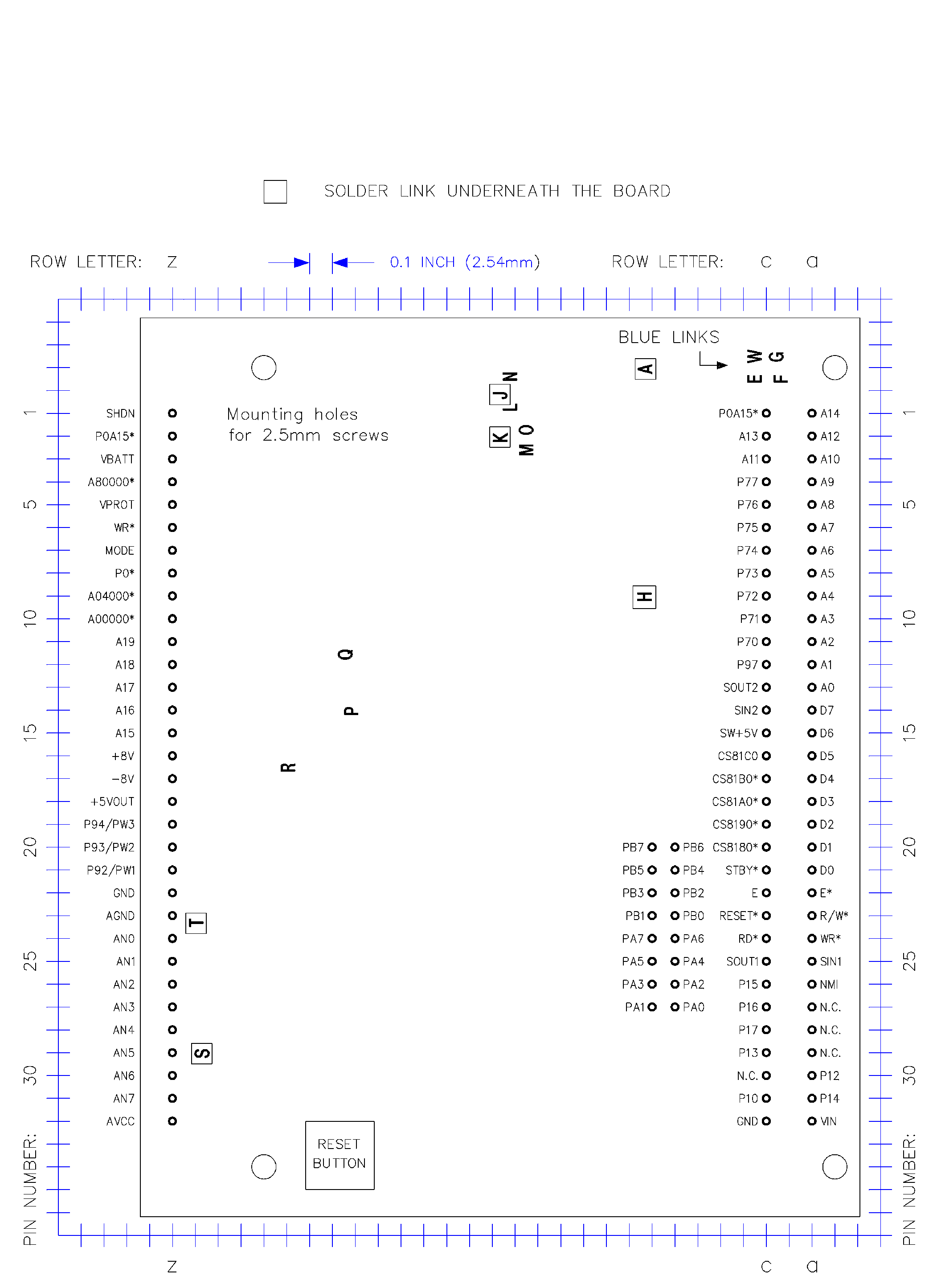
|
Pin
|
Name
|
Dir
|
Description
|
|
c1
|
P0A15*
|
Out
|
Inverted
Address bus bit 15, but logic 1 if A16 to A19 are not all 0 (i.e. not
Page 0)
|
|
c2
|
A13
|
Out
|
Address bus bit 13
|
|
c3
|
A11
|
Out
|
Address bus bit 11
|
|
c4
|
P77
|
I/O
|
Port 7 bit 7 general
purpose I/O or out pin for output compare A from timer 1
|
|
c5
|
P76
|
I/O
|
Port 7 bit 6 general
purpose I/O, or input external clock for timer 3 or out pin for output
compare B from timer 3
|
|
c6
|
P75
|
I/O
|
Port 7 bit 5 general
purpose I/O, or input external clock for timer 2 or out pin for output
compare B from timer 2
|
|
c7
|
P74
|
I/O
|
Port 7 bit 4 general
purpose I/O, or input external clock for timer 1 or out pin for output
compare B from timer 1
|
|
c8
|
P73
|
I/O
|
Port 7 bit 3 general
purpose I/O, or input pin for input capture of timer 3 or reset input for 8-bit
timer
|
|
c9
|
P72
|
I/O
|
Port 7 bit 2 general
purpose I/O or input pin for input capture of timer 2
|
|
c10
|
P71
|
I/O
|
Port 7 bit 1 general
purpose I/O or input pin for input capture of timer 1
|
|
c11
|
P70
|
I/O
|
Port 7 bit 0 general
purpose I/O or clock input for 8-bit timer
|
|
c12
|
P97
|
I/O
|
Port 9 bit 7 general
purpose I/O or serial clock in
|
|
c13
|
SOUT2
|
Out
|
Second serial port out, RS232
levels
|
|
c14
|
SIN2
|
Inp
|
Second serial port in, RS232
levels
|
|
c15
|
SW+5V
|
Out
|
Switched +5V output. Controlled
by 232ON and 232OFF .
Use to switch off other circuits to save power
|
|
c16
|
CS81C0
|
Out
|
Address 81C0-81CF decode.
Positive active, strobed with E. Use for LCDs
|
|
c17
|
CS81B0*
|
Out
|
Address 81B0-81BF decode.
Negative active, strobed with E. Do not use when keypad words INKEY or NEWKEY are
used, (needed internally)
|
|
c18
|
CS81A0*
|
Out
|
Address 81A0-81AF decode.
Negative active, not strobed with E
|
|
c19
|
CS8190*
|
Out
|
Address 8190-819F decode.
Negative active, not strobed with E
|
|
c20
|
CS8180*
|
Out
|
Address 8180-818F decode.
Negative active, not strobed with E
|
|
c21
|
STBY*
|
Inp
|
Standby input (hardware
control)
|
|
c22
|
E
|
Out
|
Clock, 1.2288MHz
|
|
c23
|
RESET*
|
I/O
|
Use as output to other logic,
or as input to reset the TDS2020F.
Use does not clear the compiled program or time and date as does power-up
|
|
c24
|
RD*
|
Out
|
Read. For Intel-style
peripherals
|
|
c25
|
SOUT1
|
Out
|
Main serial port output, RS232
levels
|
|
c26
|
P15
|
I/O
|
Port 1 bit 5 general
purpose I/O or IRQ0* interrupt i/p
|
|
c27
|
P16
|
I/O
|
Port 1 bit 6 general
purpose I/O or IRQ1* interrupt i/p
|
|
c28
|
P17
|
I/O
|
Port 1 bit 7 general
purpose I/O or 8-bit timer output
|
|
c29
|
P13
|
I/O
|
Port 1 bit 3.
Switched to 0 by 232ON and 1 by 232OFF
|
|
c30
|
|
|
Not used
|
|
c31
|
P10
|
I/O
|
Port 1 bit 0 general
purpose input, or 9.8304 MHz �-clock output
|
|
c32
|
GND
|
Gnd
|
Ground
|
|
Pin
|
Name
|
Dir
|
Description
|
|
z1
|
SHDN
|
Inp
|
Shutdown. This input must be
open circuit for correct operation. Raise it above 2.0V to close down the
TDS2020F input voltage regulator.
|
|
z2
|
P0A15*
|
Out
|
Inverted Address bus bit 15,
but logic 1 if A16 to A19 are not all 0 (i.e. not Page 0). Same as pin
c1. Duplicated so that it can be used with piggyback boards on TDS2020F.
|
|
z3
|
VBATT
|
Inp
|
Input for memory and clock
preserving battery, 2.0 to 5.8V at 3.5�A typical. The TDS2020BYN &
TDS2020BYD battery boards connect to this pin
|
|
z4
|
A80000*
|
Out
|
Address 80000-FFFFF decode.
Negative active. Used by memory expansion.
|
|
z5
|
VPROT
|
Out
|
Memory protect power supply.
Used by memory expansion piggy-back boards
|
|
z6
|
WR*
|
Out
|
Write. For Intel-style peripherals.
Same as pin a24. Duplicated so that it can be used with piggyback boards on
TDS2020F
|
|
z7
|
MODE
|
Inp
|
When open circuit H8/532
microprocessor is in Mode 4, expanded maximum mode on-chip PROM enabled. When
tied to +5V it is in Mode 3, expanded maximum mode with on-chip PROM not
enabled. Adding the TDS2020DV development piggyback board automatically ties
this to +5V and switches out the microprocessor's internal PROM.
|
|
z8
|
P0*
|
Out
|
Address 00000-0FFFF decode
(Page 0) Negative active. Used by TDS2020DV board.
|
|
z9
|
A04000*
|
Out
|
Address 04000-07FFF decode.
Negative Active. Used by TDS2020DV board.
|
|
z10
|
A00000*
|
Out
|
Address 00000-03FFF decode.
Negative Active. Used by TDS2020DV board.
|
|
z11
|
A19
|
Out
|
Address bus bit 19
|
|
z12
|
A18
|
Out
|
Address bus bit 18
|
|
z13
|
A17
|
Out
|
Address bus bit 17
|
|
z14
|
A16
|
Out
|
Address bus bit 16
|
|
z15
|
A15
|
Out
|
Address bus bit 15
|
|
z16
|
+8V
|
Out
|
Output from DC-DC converter.
Use with peripherals such as A-D
|
|
z17
|
-8V
|
Out
|
Output from DC-DC converter.
Use with peripherals such as A-D
|
|
z18
|
+5VOUT
|
Out
|
From on-card regulator. Max
100mA current including TDS2020F's
own consumption. There is also a power dissipation limit on the voltage
regulator. See POWER SUPPLY FUNCTIONS,
page 121.
|
|
z19
|
P94/PW3
|
Out
|
Port 9 bit 4 general
purpose I/O or Digital to Analog channel 3 Pulse Width Modulated output
|
|
z20
|
P93/PW2
|
Out
|
Port 9 bit 3 general
purpose I/O or Digital to Analog channel 2 Pulse Width Modulated output
|
|
z21
|
P92/PW1
|
Out
|
Port 9 bit 2 general
purpose I/O or Digital to Analog channel 1 Pulse Width Modulated output
|
|
z22
|
GND
|
Gnd
|
Ground. Same as pin c32.
Duplicated so that it can be used with piggyback boards on pin connector
version of TDS2020F.
|
|
z23
|
AGND
|
Gnd
|
Analog Ground. Cut link T to
get separate ground for A to D converter
|
|
z24
|
P80/AN0
|
Inp
|
Port 8 bit 0 general
purpose input or A to D input 0
|
|
z25
|
P81/AN1
|
Inp
|
Port 8 bit 1 general
purpose input or A to D input 1
|
|
z26
|
P82/AN2
|
Inp
|
Port 8 bit 2 general
purpose input or A to D input 2
|
|
z27
|
P83/AN3
|
Inp
|
Port 8 bit 3 general
purpose input or A to D input 3
|
|
z28
|
P84/AN4
|
Inp
|
Port 8 bit 4 general
purpose input or A to D input 4
|
|
z29
|
P85/AN5
|
Inp
|
Port 8 bit 5 general
purpose input or A to D input 5
|
|
z30
|
P86/AN6
|
Inp
|
Port 8 bit 6 general
purpose input or A to D input 6
|
|
z31
|
P87/AN7
|
Inp
|
Port 8 bit 7 general
purpose input or A to D input 7
|
|
z32
|
AVCC
|
I/O
|
Analog Reference. Cut link S if
separate reference is used for A to D converter
|
|
|
|
|
|
|
Pin
|
Name
|
Dir
|
Description
|
|
PA0
|
PA0
|
I/O
|
Port A
bit 0 general purpose I/O
|
|
PA1
|
PA1
|
I/O
|
Port A
bit 1 general purpose I/O
|
|
PA2
|
PA2
|
I/O
|
Port A bit 2 general
purpose I/O
|
|
PA3
|
PA3
|
I/O
|
Port A bit 3 general
purpose I/O
|
|
PA4
|
PA4
|
I/O
|
Port A bit 4 general
purpose I/O
|
|
PA5
|
PA5
|
I/O
|
Port A bit 5 general
purpose I/O
|
|
PA6
|
PA6
|
I/O
|
Port A bit 6 general
purpose I/O
|
|
PA7
|
PA7
|
I/O
|
Port A bit 7 general
purpose I/O
|
|
PB0
|
PB0
|
I/O
|
Port B bit 0 general
purpose I/O
|
|
PB1
|
PB1
|
I/O
|
Port B bit 1 general
purpose I/O
|
|
PB2
|
PB2
|
I/O
|
Port B bit 2 general
purpose I/O
|
|
PB3
|
PB3
|
I/O
|
Port B bit 3 general
purpose I/O
|
|
PB4
|
PB4
|
I/O
|
Port B bit 4 general
purpose I/O
|
|
PB5
|
PB5
|
I/O
|
Port B bit 5 general
purpose I/O
|
|
PB6
|
PB6
|
I/O
|
Port B bit 6 general
purpose I/O
|
|
PB7
|
PB7
|
I/O
|
Port B bit 7 general
purpose I/O
|